Hola compañeros de hive en este post quiero dar algunas nociones basicas sobre el diseño de un circuito impreso (PCB)
El diseño de PCB es una habilidad esencial para cualquier entusiasta de la electrónica. Las PCBs son fundamentales para conectar y soportar componentes electrónicos en casi todos los dispositivos modernos.
Antes de comenzar a diseñar, debes tener claros los objetivos y requisitos de tu proyecto:
1)Función del Circuito: ¿Qué debe hacer tu circuito?
2)Componentes: ¿Qué componentes necesitarás?
3)Tamaño y Forma: ¿Hay restricciones de tamaño o forma para la PCB?
a modo personal creo que lo mas importante es el tamaño y la forma de los componentes porque este tema condiciona TODO sobre como ubicarlos y como hacer las pistas y las islas.
pistas (trace): Una pista en una PCB es un camino conductor de cobre que conecta diferentes componentes electrónicos en la placa. Estas pistas permiten la transmisión de señales eléctricas y energía entre los componentes.
islas (pad): Una isla en una PCB es una pequeña área circular o cuadrada de cobre donde los componentes electrónicos se montan y se sueldan. Estas islas proporcionan un punto de conexión mecánica y eléctrica entre los componentes y la PCB.
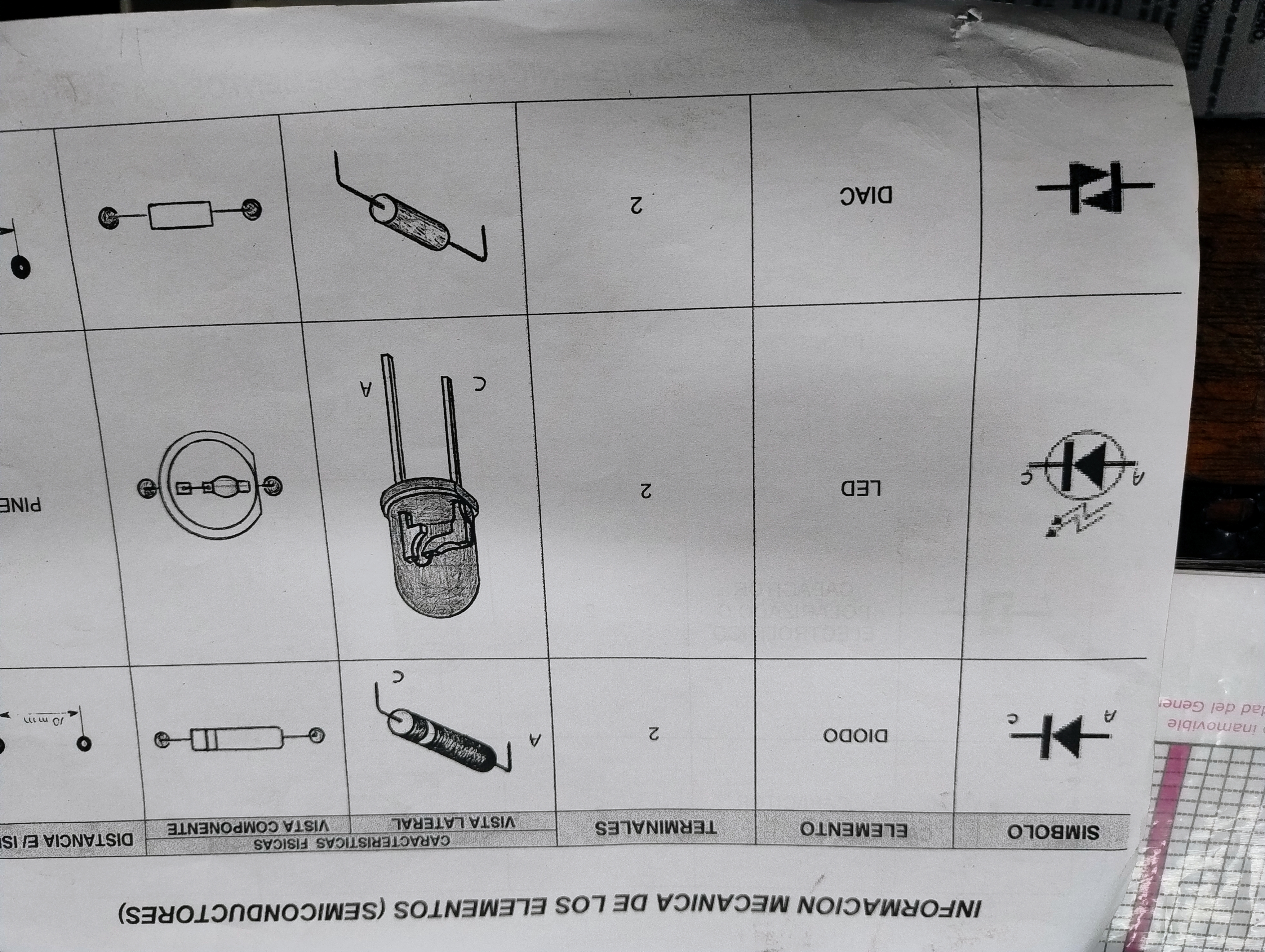
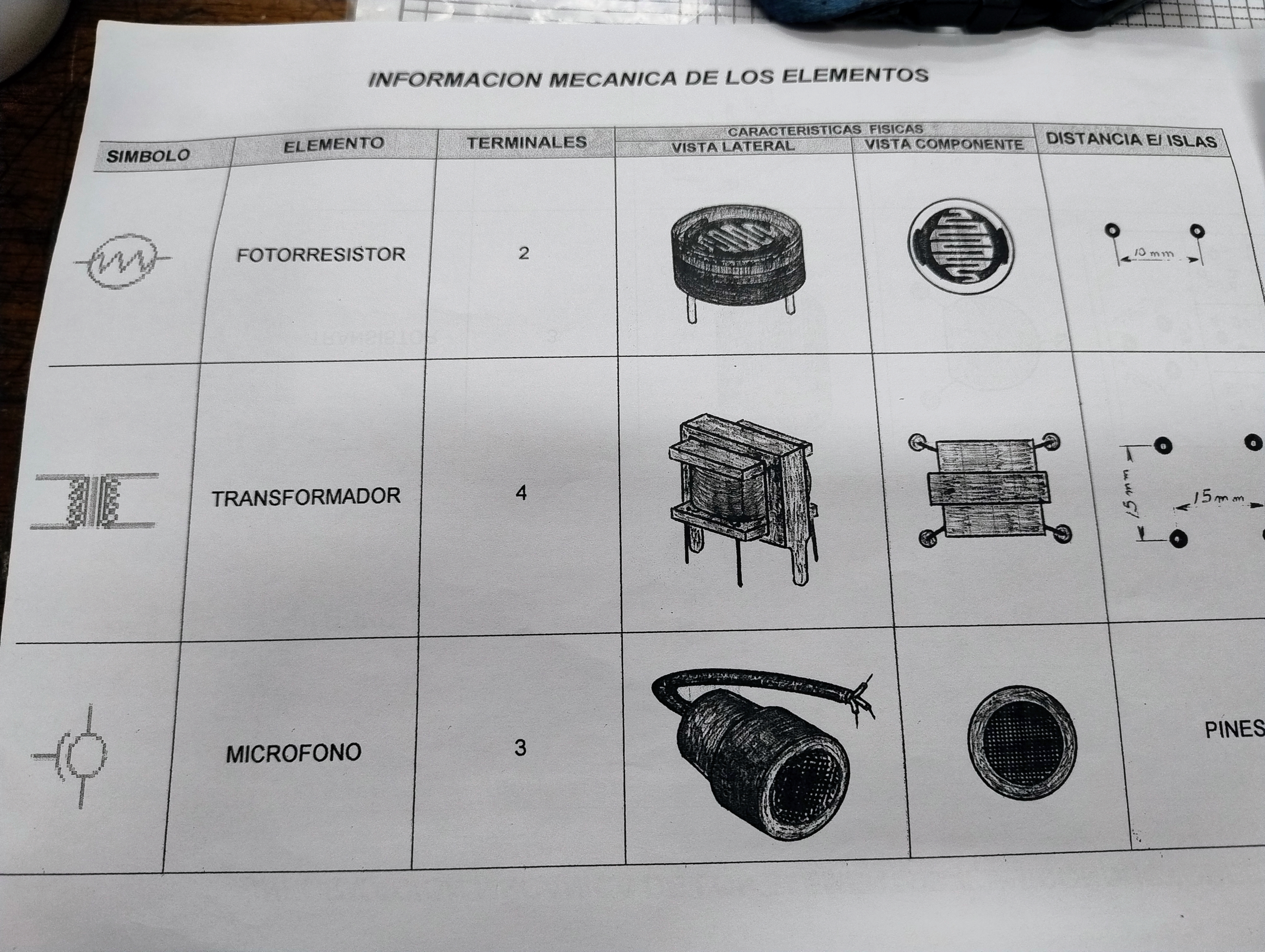
A continuación diferentes imágenes de información mecánica de componentes , como por ejemplo distancia entre ejes , símbolo eléctrico y relacion de tamaños.


Una vez que conocemos el circuito que queremos diseñar y el tipo de componentes que vamos a usar , ya podemos empezar a diseñar nuestro circuito
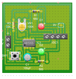
Por ejemplo yo voy a diseñar este:
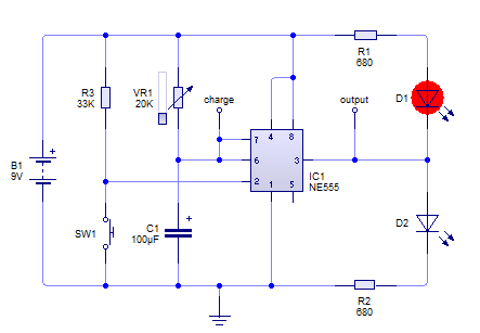
que es un 555 usado como monoestable
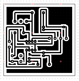
El cual logre este diseño de impreso , que puede ser asistido por computadora o también puede ser del método manual.
Y del lado de la vista de los componentes :
En el siguiente posteo voy a poner el paso a paso para lograr pasar desde el diseño hasta la plaqueta pasándola por su respectivo ataque químico hasta lograr tener la PCB terminada para que lo vean.
Un saludo compañeros de hive!
.........................................................................................
Hello hive colleagues, in this post I want to give some basic notions about the design of a printed circuit board (PCB).
PCB design is an essential skill for any electronics enthusiast. PCBs are essential for connecting and supporting electronic components in almost all modern devices.
Before starting to design, you must be clear about the objectives and requirements of your project:
1)Circuit Function: What should your circuit do?
2)Components: What components will you need?
3)Size and Shape: Are there size or shape restrictions for the PCB?
Personally, I think that the most important thing is the size and shape of the components because this issue determines EVERYTHING about how to place them and how to make the tracks and islands.
trace: A trace on a PCB is a copper conductive path that connects different electronic components on the board. These tracks allow the transmission of electrical signals and energy between components.
islands (pad): An island on a PCB is a small circular or square area of copper where electronic components are mounted and soldered. These islands provide a mechanical and electrical connection point between the components and the PCB.
Below are different images of mechanical information of components, such as distance between axles, electrical symbol and size ratio.
Once we know the circuit we want to design and the type of components we are going to use, we can start designing our circuit.
For example, I am going to design this:
which is a 555 used as a monostable
Which achieves this printed design, which can be computer-assisted or can also be manual method.
And on the component view side:
In the next post I am going to put the step by step to go from the design to the board, passing it through its respective chemical attack until I have the finished PCB for you to see.
Greetings hive colleagues!
Congratulations @tecnotronics! You have completed the following achievement on the Hive blockchain And have been rewarded with New badge(s)
Your next target is to reach 3500 upvotes.
You can view your badges on your board and compare yourself to others in the Ranking
If you no longer want to receive notifications, reply to this comment with the word
STOPCheck out our last posts:
Thanks for your contribution to the STEMsocial community. Feel free to join us on discord to get to know the rest of us!
Please consider delegating to the @stemsocial account (85% of the curation rewards are returned).
You may also include @stemsocial as a beneficiary of the rewards of this post to get a stronger support.