A team of scientists from the University of Wisconsin-Madison and the University of Wisconsin Platteville compiled transistor from carbon nanotubes. It is faster than conventional silicon transistors. This opens the way to overcome the "silicon barrier", ie the physical limitations that prevent the development of ever faster chips and more powerful computers.
Graphene nanotube [http://tech.ihned.cz]
"Transistor from carbon nanotubes, which is more efficient than silicon, represents a huge milestone," said Michael Arnold of the University of Wisconsin in Madison. "It fulfills that dream, that people engaged in nanotechnology strove for twenty years."
People behind Moore's Law
Growing performance of the computers is for decades governed by Moore's Law - which, in fact, is not the law in the true sense. In 1965, engineer Gordon Moore in a medical journal published an article in which he claimed that the number of transistors on a chip and the performance of the chip will be doubling at regular intervals. They were originally estimated at a year later the predictions of properties adjusted to 18 months.
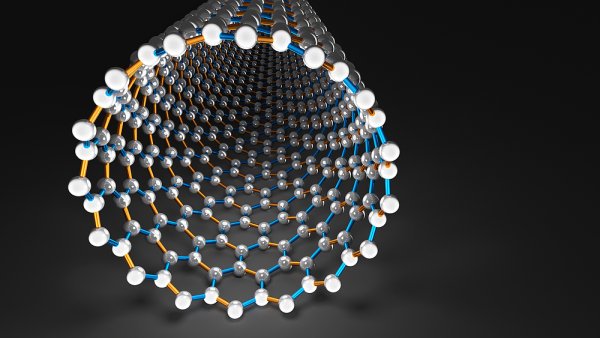
Carbon nanotubes are 50 000 times thinner than the diameter of human hair. If a human hair has the same length to diameter ratio, it would be 40 meters long. Its walls consisted of carbon atoms arranged in hexagons like a honeycomb beehive. Thus creating one atom layer, called graphene. Carbon atoms are in this embodiment interconnected extremely strong bonds, which material gives exceptional properties.
For further government to Moore's Law, in addition to the size and arrangement of the atomic structure is also important that the nanofibers can act as a transistor, which means that they can have two states. Either they are in a state of "closed" or "off" state. And more importantly, can do it better than silicon transistors. They have a much lower electrical resistance than copper, while significantly better heat dissipation. Computer simulations show characteristics of the transistors built on the basis of carbon nanotubes could be switched to five times faster than silicon or the same power consume five times less energy.
Graphene and of them coiled nanotubes represent in many ways material of dreams. Graphene layer is 100 to 200 times stronger than steel, although it is also lighter than aluminum. Carbon nanostructures for example, represent the only hope for the realization of a space elevator. Cargo into the universe should no longer be transported by rockets, but the ropes running from the base to the geostationary orbit. One atom carbon structure is also perfectly transparent, while totally impermeable to gases. And somehow incidentally also destroyed the bacteria.
For the construction of supercomputers are equally promising electrical properties of carbon nanostructures. Thanks to the slight thickness of the movement of electrons in them are governed by the laws of quantum mechanics. They seem to defy common sense. Combining graphene with other atoms and can be produced by so-called ballistic transistors, namely transistors with extremely high speed switching. The slight dimensions and other properties of graphene are likely to enable them consist of supercomputing, but very small computer chips.
So much for theory. Its conversion to life but faces many problems. So far only managed to produce microscopic scraps of graphene and nanotubes. These products are also contaminated with undesirable impurities. For the production of the transistors is on the contrary required high purity with an accurate dosing of other admixtures.
I thought that carbon tubes help to deep cool of chipset -- to produce 3D chips. Today they all are 2D (but it may be several layers).
In fact, Intel uses 3D transistors right now for skylake
Does it mean that some part of skylake chipset is 3D and we cannot "draw the circuit on plane"?
No, that means that chipset is 2D, but transistors are "3D" http://www.cnet.com/news/how-intels-3d-tech-redefines-the-transistor-faq/
Source: http://tech.ihned.cz/c1-65428090-vedci-sestavili-tranzistor-z-uhlikove-nanotrubice-cipy-z-uhliku-maji-byt-vyrazne-vykonnejsi-nez-kremikove
Not citing sources is plagiarism, and copying pasting articles without permission is copyright infringement. If you want to share a news story, simply link to the source, and include your original commentary, and possibly small quotes from the source.
Copy paste is discouraged by the community, and may result in action from the cheetah bot.
Creative Commons: If you are reposting under a Creative Commons license, please attribute and link according to the specific license. If you are reposting under CC0 please consider noting that at the end of your post.
If you are actually the original author, please do reply to let us know!
Thank You! ☙
Thanks for pointing that out. Thought that citing picture is as I cite all article. Will study more about CC and follow the rules. I translated it ( no C+P ;), you can see many mistakes there :(
Sorry.