To study well is to set goals in life. To study is to gain knowledge and impart it to others.
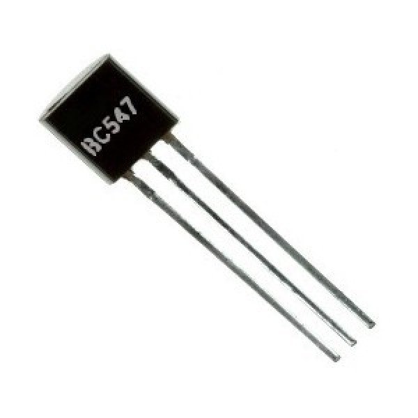
Good Day Steemians! Today, I'll give you guys an overview about the one of the most known electronic component, the Bipolar Junction Transistor.

Source: Google
•History
On December 23, 1947, electronics industry starts to make steps to experience the advent to a completely new direction of interest and development. Afternoon that day, Walter Brattain, William Shockley and John Bardeen demonstrated the amplifying action of the first ever transistor named Point-Contact Transistor made at Bell Telephone Laboratories.
•Construction

Source: Google
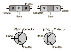
A transistor is a three-layer semiconductor device that has two negative-type and one positive-type material or two positive-type and one negative type material. A transistor with two negative-type material with one positive type material in between is called as NPN transistor and the one with two positive-type material with one negative-type material in between is called PNP transistor. Obviously, it is named based on the order of materials. A transistor has three pins, the emitter, collector and base.
•Operation
.png)
Source: Google
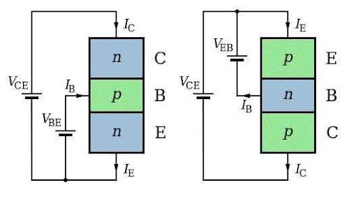
The name Bipolar Junction Transistor was made to the fact that there's two polarity runs in the transistor, the electron (negative polarity) and holes (positive polarity). The photo above shows the flow of both polarity and proper biasing of transistor. Proper biasing must be observed to achieve the primary function of BJT(Bipolar Junction Transistor), to amplify. To proper bias the NPN transistor, the negative side of the voltage source V1 must be connected to the emitter pin of the transistor and the positive side of voltage source V1 must be connected to collector pin. The positive side of another voltage source V2 must be connected to the base pin and the positive side of voltage source V2 must be connected to the colletor pin(refer picture below).
.jpeg)
Source: Google
BJT is so governed by current and there's 3 kinds of current that flows around the BJT. The Ie ( the current that flows in the emitter side of transistor), Ib (the current that passes through the base) and the Ic ( the current that passes through the collector.
.png)
Source: Google
The invention of transistor, the point-contact transitor specifically, was a Nobel Prize in the year 1956. This invention really gives a big contribution to today's modern life especially in the electronics industry.
I hope that you gain something from my post. Feel free to comment down some question related to the post. I'll the my best to answer your questions.
That's all for today. Have a great day ahead everyone. God Bless!
-renatoaying-
Wow. This is very useful for us in knowing deeper about transistor keep steeming
Yeah I will :) Keep steeming as well :)
You can use this tool to easily give credit to the sources of your images https://steemitcuration.appspot.com/imageformat .
Thank you so much for the tip. I appreciate it so much :)
Thanks for this information.
My pleasure :)
very good post dong...
plus 100 😊
Hehe :) Thank you maam :)
I love the Electronics world <3
Really? Good to hear that :)
Hi there!!! It's my pleasure to meet you :) very helpful in @steemitcommunity :) to nourish unique talents like you did :)
Nice to meet you too :)